


表面粗さを理解する
著者: Victoria Marcune,Shawn Iles
表面粗さは、表面の形状が理想的な形状からどの程度逸脱しているかを表す要素の一つで、値が大きくなるほど表面が粗くなり、小さいほど表面が滑らかになります。粗さは、オングストローム (10-10 m) オーダーの微小な偏差となり、高空間周波数での誤差を表します。散乱は、光学部品の面粗さに比例して大きくなるため、光学面の表面粗さを理解することは、光の散乱を制御する上で極めて重要になります。表面粗さによる光の散乱と吸収は、ハイパワーレーザーシステムなどのアプリケーションにおいて多大な影響を及ぼし、効率やレーザー損傷閾値に負の影響を与えることがあります。損傷閾値への影響に加えて、ハイパワーレーザー放射の散乱は、予期せぬ方向に光が向かってしまうことから、システムの周辺で作業する人にとって安全上の危険要素になる可能性があります。表面粗さに利用される現在の標準規格 ISO 10110-8 は、表面粗さをどのように分析・規定するかについて定義しています。
表面粗さの数値を読み取る
ISO 10110-8に準拠した図面では、光学面の完全な描写を与える以下の仕様が記載されます。
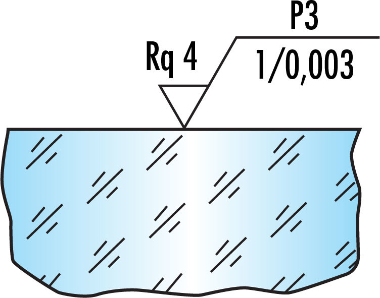
Figure 1: 表面粗さの仕様例
表面仕上げは、Figure 1では「P3」で示されています。
この変数は表面仕上げを表します。単純な研磨仕様の場合、砂面 (ground surface) を示す「G」か、光学研磨 (polished surface) を示す「P」のどちらかになります。研磨のグレードは、以下のTable 1に示す、10mmスキャン当たりの微小欠陥数に関する滑らかさの度合に応じて1-4までの等級に割り当てられます。
| 研磨グレード | サンプリング長10mm当たりの微小欠陥数、N |
|---|---|
| P1 | 80 ≤ N < 400 |
| P2 | 16 ≤ N < 80 |
| P3 | 3 ≤ 16 |
| P4 | N < 3 |
Table 1: 微小欠陥に関する滑らかさの指標
使用した統計学的手法は、Figure 1では「Rq 4」で示されています。
これは、表面粗さの測定に用いられた統計学的手法を表し、数値がその後に続きます。
空間帯域幅は、Figure 1では「1/0.003」で示されています。
これは、空間帯域幅の上限から下限までを表します。
空間周波数と周波数グループ
光学部品の表面テクスチャを定量化する場合、どのレベルの空間分解能で測定するのかを定義することが重要です。表面テクスチャ、つまり表面の完全な形状は、粗さ (roughness)、うねり (waviness)、および形状 (figure) の3つの主要な空間周波数グループに分けることができます。

Figure 2: 形状、うねり、および粗さは、異なるスケールでの表面テクスチャを特徴付ける
Figure 2は、表面の形状、うねり、および粗さが、その理想的な形状からどのように逸脱しているかを示します。形状は、表面の全体的形状を表し、分析される最大スケール、すなわち最大の空間周波数になります。形状 (figure) によって表される誤差は、数十分の1mmからcmのオーダーです。うねり (waviness) は、μmからmmオーダーでの特徴を表す中空間周波数での誤差を表します。粗さ (roughness) は、誤差の中でも最も小さくなり、数十分の1オングストロームから数十分の1μmオーダーでの表面テクスチャの異常さを表します。
ISO 10110-8 表面粗さパラメータ
ISO 10110-8の目的は、表面テクスチャの定義方法を規定することです。ISOによると、表面粗さは、「統計学的手法を用いて効果的に表すことができる面の特性」となります。ISO規格は、光学的に滑らかな表面を表すために用いられる5つの統計学的手法を概説しています。これらの方法は、組み合わせて使うことも、さまざまな空間帯域幅で使うこともできます。正確な結果を得るためには、空間周波数の上限と下限を定義することが極めて重要になります。空間周波数が定義されていない場合、ISO 10110-8規格では0.0025mm – 0.08mmまでの範囲を想定して規格化することになります。
1 & 2. RMS粗さとうねり:光学的に滑らかな面を規定する最も一般的な方法は、米国では二乗平均平方根 (RMS) 法になるのに対して、欧州では絶対的粗さになります。平均線からの高さ偏差のRMS平均は、光学面の滑らかさを統計学的に分析するのに利用されます。RMS粗さ (Rq) は、粗さの分布を指すのに対し、RMSうねり (Wq) は、うねりの分布を指します。どちらも同じRMS法で測定されますが、異なる空間周波数で測定されます。
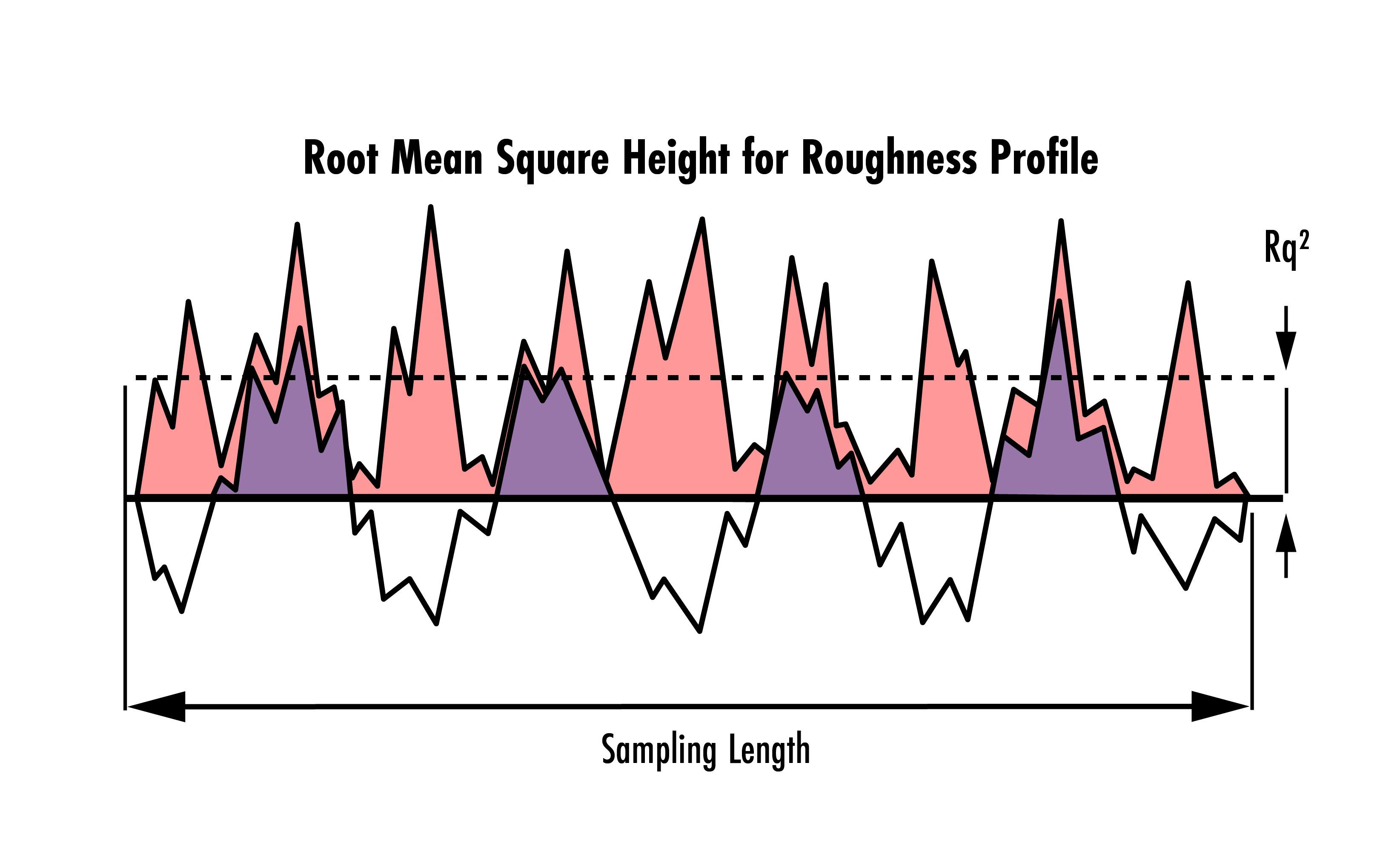
Figure 3: 与えられたサンプル長に対して測定される粗さ分布の例。Rq2は二乗平均平方根の高さを表す
3. RMSスロープ:光学的に滑らかな面は、RMS粗さやうねりと同様、与えられたサンプリング長に沿った面の局所的な傾き、$ \tfrac{\text{d} Z \left( x \right)}{\text{d}x} $ のRMSスロープを用いて規定することができます。
$$ \begin{pmatrix} T\\ T \Delta q \end{pmatrix} = \begin{Bmatrix} \begin{pmatrix} Rq\\ R \Delta q \end{pmatrix} \text { for } 1 \large{\unicode[computer modern]{x212B}} \leq lr\leq 1 \large{\unicode[computer modern]{x03BC}} \normalsize{\text{m}} \\ \begin{pmatrix} Wq\\ W \Delta q \end{pmatrix} \text { for } 1 \large{\unicode[computer modern]{x03BC}} \normalsize{\text{m}} < lr\leq 1 \text{mm} \end{Bmatrix} $$
$$ \begin{pmatrix} T\\ T \Delta q \end{pmatrix} = \begin{Bmatrix} \begin{pmatrix} Rq\\ R \Delta q \end{pmatrix} \text { for } 1 \large{\unicode[computer modern]{x212B}} \leq lr\leq 1 \large{\unicode[computer modern]{x03BC}} \normalsize{\text{m}} \\ \begin{pmatrix} Wq\\ W \Delta q \end{pmatrix} \text { for } 1 \large{\unicode[computer modern]{x03BC}} \normalsize{\text{m}} < lr\leq 1 \text{mm} \end{Bmatrix} $$
(完全な方程式を見る場合は、右にスクロールしてください)
4. 微小欠陥の密度の指定:微小欠陥とは、光学的に滑らかな面に見られる窪みやキズのことです。一般的には、光学式プロファイロメーター、顕微鏡、あるいは顕微鏡画像コンパレータを用いて定量化されます。ISO 10110-8では、「微小欠陥の数 $ N $ を10mmラインスキャンにわたり3µmの分解能、あるいは300µm $ \times $ 300µmのエリアを同じ分解能でカウントする」と規定しています。
5. パワースペクトル密度 (PSD) 関数:PSD関数は、表面粗さを測定するための最も包括的な統計学的手法の一つです。これは、各粗さ成分の相対的分布を空間周波数の関数として定量化することで、表面テクスチャ特性の完全な描写を可能にします。
(完全な方程式を見る場合は、右にスクロールしてください)
これは2次元曲面のPSDを計算するのに用いられる一般的な式です。$ f_x $と$ f_y $は、表面のテクスチャ$ z \!\left( x, y \right) $ の空間周波数になり、一辺の長さ $ L $ のエリア上で定義されます。
表面粗さを測定するための計測技法
さまざまな空間周波数に合わせた、一連の計測技法があります。最も一般的なものは、従来型干渉計、白色光干渉計、および原子間力顕微鏡です。以下のFigure 4は、これらの技法に最適な領域と波長を示します。
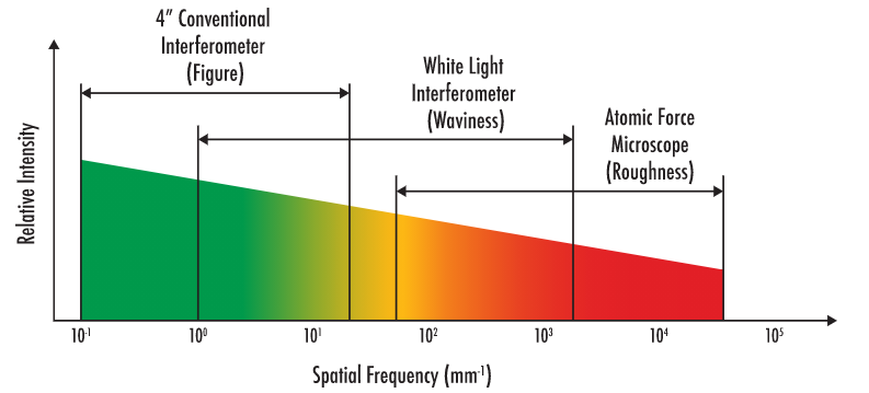
Figure 4: 代表的な計測機器の空間周波数領域
従来型の干渉計は、低空間周波数誤差を測定するのに最適です。このクラスに属する表面誤差は形状誤差と呼ばれ、典型的なゼルニケ多項式で関連付けられます。ゼルニケ多項式は、光学部品がその理想的形状から逸脱した時に起こる波面収差で生じる誤差を表します。白色光干渉計は、うねり、あるいは中空間周波数誤差を測定するのに最適です。うねりは、ヘイジングやコントラスト低下といった効果を生み出す要因となります。最後に、原子間力顕微鏡は、光学面の粗さを特徴付ける高空間周波数誤差に対し、最高の分解能を提供します。白色光干渉計と原子間力顕微鏡は、粗さ測定に使用できるため、これらのグループ内で重複する部分もあります。装置の正しい選択は、アプリケーションの波長に部分的に依存します。例えば、可視またはIRスペクトルを測定する場合、一般的に2,000サイクル/mm未満の周波数で分析されるため、白色光干渉計が理想的になります。
超短パルス用光学部品の表面品質を規定する
超短パルス用光学部品を分析する時、表面品質を規定する標準化が現時点で行われていないことから、メーカーが独自の裁量でそれを行っています。超短パルス用光学部品メーカーの何社かではコーティング前の表面品質のみを規定しているのに対し、他のメーカーではコーティング後の表面品質を20-10かそれ以上の仕様で行っています。
超短パルスアプリケーション用に作られる光学部品は、長いスパッタリング工程を要する厚くて特殊なコーティングを通常特徴としています。この工程の長さにより、欠陥がコーティング中にスパッタリングされ、外観上の「ダスト」や不規則な表面品質につながります。このような欠陥は、ダストというより、スパッタされる材料のフロー中に起こる小さなサージで生じます。コーティングプロセス中、スパッタリングレートにばらつきが生じることがあり、その結果、コーティングの局所的な微小析出が起こります。
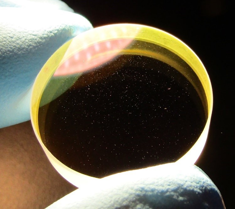
Figure 5: 超短パルス用コーティングを施した光学部品の代表的な外観。不規則な表面品質の外観にもかかわらず、エドモンド・オプティクスは、自社の超短パルス用光学部品の規定した性能を保証します。
その外観品質にもかかわらず、こうした欠陥は光学部品の全体性能にほとんど影響を与えません。これらの欠陥のサイズは比較的小さいため、群遅延分散や反射率などのフィルムのバルク特性を考慮すると、ビームの影響を受ける部分は大きくありません。大抵の状況で無視できますが、小さなビームサイズや超低損失を求めるアプリケーションでは、このような欠陥によるシステム内の散乱の増加が無視できなくなる可能性があります。より厳しい仕様に適合するために、スーパーポリッシュ基板を用いて散乱を全体的に減少させるなど、特別な措置を取る場合があります。
エドモンド・オプティクスでの計測
製造するものを測定することは製造の重要な要素です。エドモンド・オプティクスは、部品が規定された要件に適合することを保証するために、厳格なグローバル品質プログラムを利用しています。干渉計、プロファイロメーター、三次元測定機 (CMM)、そしてその他の多くの光学的・機械的計測機器をはじめとした一連の装置が、表面粗さやその他の光学的特性を社内テストで測定するために利用されています。当社の固有の計測対応力の詳細は、計測対応力のウェブページをご覧ください。
参考文献
- ISO 10110-8:2019, Optics and photonics — Preparation of drawings for optical elements and systems — Part 8: Surface texture
- Filhaber, John. “LARGE OPTICS: Mid-Spatial-Frequency Errors: The Hidden Culprit of Poor Optical Performance.” Laser Focus World, 13 Aug. 2013
- “Root Mean Square Slope (Rδq, Pδq, Wδq): Surface Roughness Parameters.” Root Mean Square Slope (Rδq, Pδq, Wδq) | Surface Roughness Parameters | Introduction To Roughness | KEYENCE America
- Deck, Leslie L., and Chris Evans. “High Performance Fizeau and Scanning White-Light Interferometers for Mid-Spatial Frequency Optical Testing of Free-Form Optics.” Advances in Metrology for X-Ray and EUV Optics, 2005, https://doi.org/10.1117/12.616874.
- Jayson Nelson, Shawn Iles, "Creating sub angstrom surfaces on planar and spherical substrates," Proc. SPIE 11175, Optifab 2019, 1117505 (15 November 2019); https://doi.org/10.1117/12.2536689


もしくは 現地オフィス一覧をご覧ください
クイック見積りツール
商品コードを入力して開始しましょう
Copyright 2023, エドモンド・オプティクス・ジャパン株式会社
[東京オフィス] 〒113-0021 東京都文京区本駒込2-29-24 パシフィックスクエア千石 4F
[秋田工場] 〒012-0801 秋田県湯沢市岩崎字壇ノ上3番地
The FUTURE Depends On Optics®